
ASML
ASML Holding NV
What's Their Growth Strategy?
What's Their Growth Strategy?First part company self understanding:
We’ll continue to enable many of the solutions that are transforming our planet.”
Christophe Fouquet
President, Chief Executive Officer and Chair of the
Board of Management (annual report 2024)
Examples of strategy and selfview (for more info see anual reports):
ASML – self-understanding & growth narrative summarized:
Purpose (why they exist):
ASML exists to enable human progress. Since its founding in 1984, the company has pursued one central aim: to push the boundaries of semiconductor technology and help solve some of society’s toughest challenges. By empowering the production of advanced chips, ASML makes breakthroughs in AI, healthcare, communications, energy efficiency, and sustainability possible.
ASML sees itself not as a machine maker, but as the enabler of global innovation.
Vision (What they strive to achieve):
ASML’s vision is to unlock human and societal potential by extending the limits of technology.
This means:
Driving Moore’s Law forward through advanced lithography.
Making ever-smaller, more powerful, and more energy-efficient chips feasible.
Creating the technological foundation for the digital economy, from cloud & AI to autonomous driving and medical technology.
-> In ASML’s vision, every leap in chipmaking translates into a leap for society.
Mission (What they uniquely do):
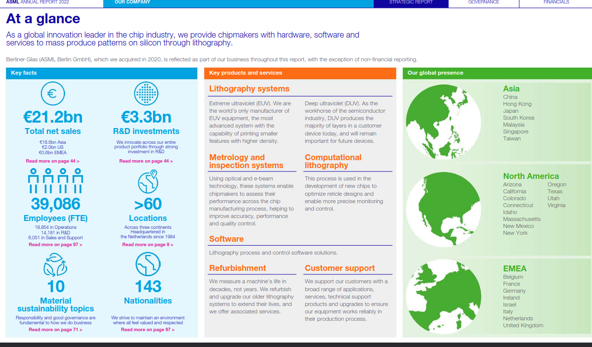
ASML is the only company worldwide to provide a holistic lithography ecosystem, combining:
Hardware – cutting-edge EUV & DUV lithography systems.
Software & computational tools – enabling chip design optimization and predictive yield improvement.
Metrology & inspection – ensuring precision, accuracy, and control at atomic scales.
Process control solutions – maximizing chipmakers’ performance, yield, and cost efficiency.
-> No competitor offers such an integrated end-to-end patterning platform – this is ASML’s unique edge.
Core Values Driving Growth (How they act):
We challenge → We question the status quo, pushing boundaries in physics, engineering, and business.
We collaborate → We work in deep partnership with customers, suppliers, governments, and academia to co-develop the future.
We care → We act with integrity, inclusivity, and respect. We develop talent, nurture diversity, and safeguard a sustainable future.
-> These values guide ASML in balancing innovation, collaboration, and responsibility – ensuring resilience and long-term growth.
Conclusion:
ASML frames itself as the indispensable system integrator of the semiconductor industry.
Its purpose is progress, its Vision is human potential unlocked, its Mission is the holistic lithography ecosystem, and its Core Values are the cultural engine that turns strategy into execution.
Second part - is the story they tell true? - a critical look :
ASML – Strategy, Technology & Growth Outlook (2025–2030)
Mission & Self-Image (reminder)
Purpose: “Unlocking the potential of people and society by pushing technology to new limits.”
Mission: Sole provider of a holistic lithography ecosystem (EUV/DUV hardware + software + metrology + process control).
Values: Challenge, Collaborate, Care → innovation, deep ecosystem partnerships, and responsible leadership.
Growth & Market Outlook analysis:
AI as main growth driver: CEO Christophe Fouquet highlights AI as a “major market shift” and the key growth driver in 2025.
Demand from hyperscalers and AI giants investing heavily in infrastructure.
Two-speed market:
AI-related customers are highly optimistic and even signal upside potential.
Other non-AI segments remain more cautious, creating short-term uncertainty for 2025.
Order backlog ~€36B supports strong visibility into 2025.
China: Strong in 2023/24 due to backlog clearing, expected to normalize going forward.
Industry CAGR ~9% (2025–2030) → semiconductor market >$1T by 2030.
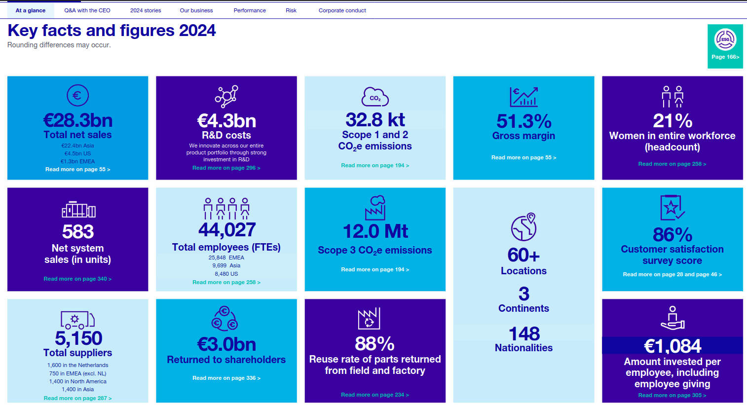
ASML targets: €44–60B revenue and 56–60% gross margin by 2030.
Technology & Moore’s Law- how long will it go on? - for years to come:
Moore’s Law continues through both 2D scaling + 3D integration, in the sense that transistor density doubles every two years
possible increasing instead of doubling to 16x every two years in the near future
EUV (13.5 nm, 0.33 NA): standard for advanced <7nm nodes.
High-NA EUV (0.55 NA): next leap, 8nm resolution, enabling ~1nm nodes; ramping into high-volume manufacturing ~2025.
3D NAND: scaling from 176 layers (2024) → >600 layers (2030).
Cost factor: CEO stresses lithography advances not only boost performance but lower costs per transistor → expands AI adoption into everyday devices (PCs, smartphones).
Timeline clarity: CEO explicitly says Moore’s Law has at least two more decades of innovation runway -> not unlikely by considering all technical aspects for improvement
Scale of EUV logistics: The fact each machine requires multiple planes/trucks underlines barriers to entry and uniqueness.
Structural driver: AI framed as not just a growth engine for 2025, but as a 20-year technology pull for advanced lithography.
Patience as moat: Highlights how ASML’s willingness to invest for decades differentiates it culturally and strategically.
EUV core process – the technological moat:
50,000× per second process:
Tiny tin droplet (30 µm) injected into vacuum chamber.
Weak laser pulse flattens it into a “pancake”.
Strong laser pulse vaporizes it into plasma 40× hotter than the sun’s surface.
Plasma emits broad-spectrum light with a peak at 13.5 nm (EUV).
Collector mirror focuses EUV into the lithography system for wafer exposure.
Importance:
Result of decades of R&D → extremely complex, near-impossible to copy.
Basis for advanced chips <7nm, required for AI and high-performance computing.
High productivity (wafers/hour) underpins ASML’s revenue forecasts and backlog.
Risks:
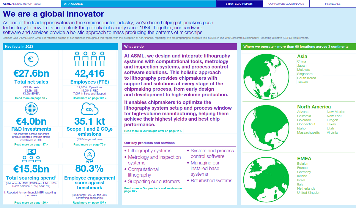
Geopolitics: Export controls (China ~36% of 2024 sales), Taiwan/Korea tensions.
Supply chain: Heavy reliance on single suppliers (e.g., Zeiss optics); material availability risks.
Operational: High-NA ramp highly complex; long lead times; customer concentration.
Financial: Semiconductor cycles, FX (EUR/USD), inflation, tax changes.
ESG: Net-zero by 2040, Scope 3 targets depend on suppliers; potential regulatory burden.
Cybersecurity: Increasing attacks; AI/quantum may amplify threat.
Investments & Partnerships:
R&D spend ~€5B/year (~15% of revenue).
New factories & expansions (e.g., $300M Wilton, USA +1,000 jobs).
Equity investment: €1.3B lead stake in Mistral AI → integrating AI in ASML systems.
Academic/research ties: imec, TU/e, ARCNL, >180 global universities.
Public-private programs: EU Chips Act, High-NA EUV lab (with imec).
Capital return: Dividends (€6.40/share 2024) + ~€3B/year share buybacks.
Management & Culture:
CEO Christophe Fouquet: “Very bullish” through 2030, while warning of macro/geopolitical uncertainty in 2026.
CFO Roger Dassen: Emphasizes cautious near-term but long-term secular growth.
Culture priorities: Ownership + Simplification → faster innovation and execution.
Diversity & Inclusion: Highlighted as drivers of creativity and scaling.
Technology Pipeline & Innovation:
Innovation funnel: Idea → Proof-of-concept → Engineering → Full systems.
ASML Fellowship Program to recognize top technical leaders.
R&D focus: higher EUV source power, improved energy efficiency, robust wafer handling, 3D IC integration.
Long-term roadmap: extend High-NA EUV, research beyond EUV, advanced metrology and packaging.
Conclusion - It's true:
Moat: Unmatched monopoly on EUV/High-NA + ultra-complex tin-plasma EUV process.
Growth: Driven by AI megatrend, supported by Moore’s Law (2D+3D), and large backlog.
Risks: Mainly geopolitical (China/Taiwan), supply-chain concentration, and execution.
Capital allocation: Balanced between heavy R&D, capacity build out, and shareholder returns.
Bottom line: ASML is the “indispensable bottleneck” of the semiconductor industry, combining monopoly-grade technology with secular growth tailwinds.
Deeper technology Analysis and comparison to other companies:
Current Leadership
ASML is the only EUV supplier worldwide; Nikon exited EUV because it's to expensive, Canon focuses on NIL, China remains behind stuck at 28nm tech
EUV already indispensable for <7 nm logic & DRAM fabs .
Each EUV tool is extremely complex (100,000+ parts, logistics need multiple planes/trucks)
Roadmap & Moore’s Law
0.33 NA EUV (NXE) → mature, used in 5–7 nm production .
0.55 NA High-NA EUV (EXE) shipped in 2023, ramping 2024–25 → enables ≈8 nm critical dimensions, ~2 nm logic nodes NA (≥0.7) under exploration; engineering and cost challenges huge .
ASML claims EUV scaling can support ~1 nm node by ~2030–2033
RDS (2023) notes Moore’s Law pace continues but with more emphasis on 3D integration & system scaling after ~2028
Technical & Economic Challenges
High-NA EUV faces stochastic defects, mask complexity, thin resists .
Each new node shows diminishing cost-per-transistor gains (~10–20% vs. historic 35–40%) .
High-NA field size smaller → more exposures per wafer; ASML compensates with faster stages (~220 wafers/hour)
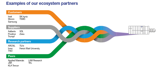
Partnerships & Ecosystem
ZEISS optics: sole supplier; ASML owns 24.9% stake, co-invested €1.5B+ built High-NA optics (10M man-hours, 12 ton assemblies, 40,000+ parts)
Imec partnership (2024–25): sub-2 nm R&D pilot line with ASML’s full product range, EU-funded
TU/e collaboration: €80M over 10 years to train PhDs in optics, plasma
Canon NIL: showed ~2 nm demo, but yields/measures far behind ASML .
China: SMEE developing DUV/EUV but far from production-grade systems; local reports admit years of gap for no no compeditor is close
Financial & Market Support
R&D: €4–5 B/year (~15% revenue); €1.2B per quarter
gross margins ~50–55% allow self-funding + dividends/buybacks .
AI demand: >80% of 2024 logic system sales serving AI chipmakers Act & U.S. CHIPS Act funnel subsidies into fabs (TSMC, Intel, Samsung) → indirect support for ASML .
Long-Term Outlook:
Near-term (2024–2026): High-NA EUV ramping; Moore’s Law scaling continues to ~2 nm
(2026-2030): UV + 3D stacking sustain Moore’s Law to ~1 nm
2030: Scaling slows; IRDS projects pivot to 3D architectures & system scaling, Global semiconductor progress effectively hinges on ASML’s roadmap
Evidence strongly suggests ASML will remain unrivaled in EUV through at least 2030–2033, enabling Moore’s Law down to ~1 nm. Barriers: massive IP portfolio, exclusive ZEISS partnership, heavy R&D, and customer lock-in.
Risks: economics (tool cost), technical challenges (defects, masks), and geopolitics (export bans, China).
Summary of everything and final conclusion - ASML growth strategy for the future:
Pushing Moore’s Law: Advancing with High-NA EUV while continuing DUV sales as dependable “cash cows.”
Holistic Ecosystem Lock-In: Software, metrology, and process control solutions that bind customers across the entire production chain.
Fab Optimization: Squeezing every bit of efficiency and yield out of fabs.
Service & Upgrades: Extending machine lifetimes and creating recurring revenue streams.
High R&D Intensity: Reinvesting 15–18% of revenue to widen the moat and maintain technological leadership.
Deep Alliances: Long-term partnerships with TSMC, Intel, Samsung, and IMEC.
AI Integration: Leveraging artificial intelligence to optimize chip design and manufacturing processes.
Cash Generation & Pricing Power: Strong margins supported by unique technology and irreplaceable positioning.
Margin-Rich Service Contracts: Ensuring stability across cycles with predictable, recurring income.
Mission-Driven Culture: Purpose-led identity that strengthens long-term focus and exceptionally managment which reenforces this identity
Talent Magnet: Recruiting the world’s top physicists and engineers — attracting talent competitors like Nikon and Canon simply cannot.
Please let me know if I’ve missed or overlooked anything, made a mistake, or if you have any questions or suggestions for improving the analysis!
sources:
https://www.asml.com/en/investors/why-invest-in-asml/financial-strategy
https://www.asml.com/en/investors/investor-days/2024
https://www.asml.com/en/investors/annual-report
https://www.asml.com/en/investors
https://www.reuters.com/technology/asml-ceo-says-ai-boom-benefits-company-2024-11-14
https://www.semiconductor-digest.com/moores-law-indeed-stopped-at-28nm/
https://en.wikipedia.org/wiki/Moore%27s_law
https://irds.ieee.org/images/files/pdf/2022/2022IRDS_Litho.pdf
https://nvlpubs.nist.gov/nistpubs/SpecialPublications/NIST.SP.1500-208.pdf
https://semiengineering.com/high-na-euv-complicates-euv-photomask-future
https://arxiv.org/abs/2402.18234
https://arxiv.org/abs/2506.15558
https://arxiv.org/abs/2508.00433
https://en.wikipedia.org/wiki/Multiple_patterning
https://www.asml.com/en/news/stories/2024/5-things-high-na-euv
https://www.electrooptics.com/feature/future-euv-lithography
Interviews with ASML people and videos: